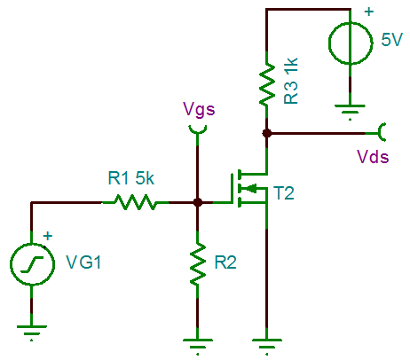
The following diagram shows an NMOS switching circuit. The step signal VG1 is set to a DC level of 2V, square wave (amplitude 2V, frequency 50Hz), and the turn-on voltage of T2 is 2V. Therefore, the MOSFET T2 will switch between the on and off states with a period of T=20ms.
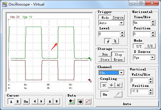
Firstly, by simulating the waveforms of Vgs and Vds, one can see a small platform when Vgs=2V. Some people may wonder why Vgs has a small platform when it rises?

MOSFET Vgs Mini Platform
Improvement in MOSFET Vgs small platform
To understand this phenomenon, theoretical knowledge is needed to support it.
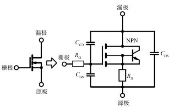
The Equivalent Model of MOSFETs
The MOS transistor pattern we usually see is the one on the left, and the one on the right is called the equivalent model of the MOS transistor.
Among them: Cgs is called GS parasitic capacitance, Cgd is called GD parasitic capacitance, input capacitance Ciss=Cgs+Cgd, output capacitance Coss=Cgd+Cds, reverse transmission capacitance Crss=Cgd, also known as Miller capacitance.
If you are not familiar with the concept of MOSFET input/output capacitance, please click: to help you understand the MOSFET parameters "thermal resistance, input/output capacitance, and switching time"
The main culprit of the Miller effect is the Miller capacitance, which refers to the effect of amplifying the equivalent input capacitance value by the distributed capacitance Cgd between its input and output under the effect of inverse amplification. The Miller effect forms the Miller platform.
Firstly, one thing we need to know is that due to the manufacturing process of MOSFETs, Cgd is inevitably generated, which means that Miller capacitance must exist, so the Miller effect is inevitable.
So, what are the drawbacks of the Miller effect?
The opening of MOSFETs is a process from scratch, and the longer the overlap time between the D and S poles of MOSFETs, the greater the conduction loss of MOSFETs. Due to the presence of Miller capacitors and Miller platforms, the turn-on time of MOSFETs increases, and the conduction loss of MOSFETs is bound to increase.
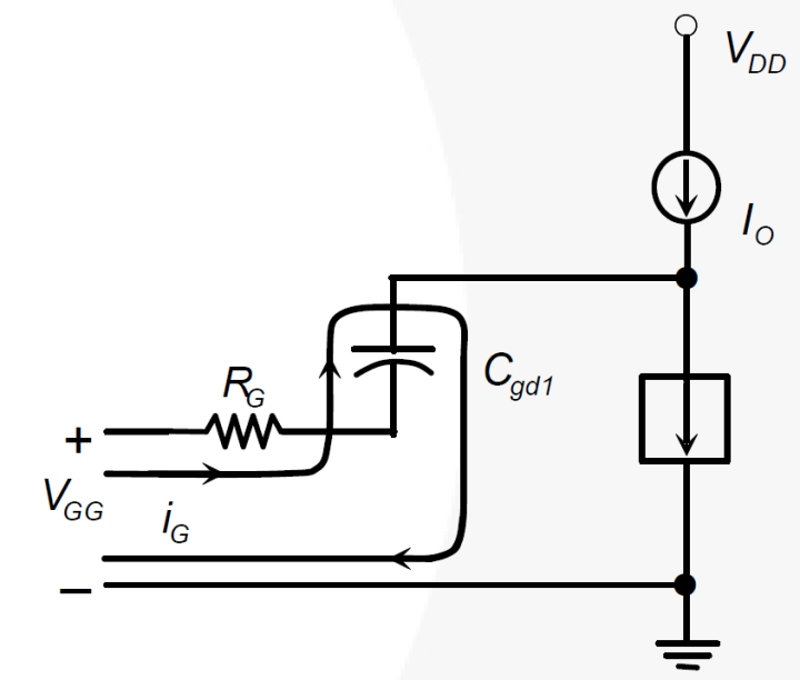
After reducing the G-pole resistance R1 during simulation, we found that the Miller platform has improved? We should all know the reason.
The opening of the MOS transistor can be seen as the charging process of the parasitic capacitor Cgs by the input voltage passing through the gate resistance R1. The smaller R1, the faster Cgs charges, and the faster the MOS transistor opens. This is the reason why the Miller platform has improved by reducing the gate resistance.
What exactly happened on the Miller platform?
For NMOS transistors, before the MOS transistor is turned on, the D-pole voltage is greater than the G-pole voltage. As the input voltage increases, Vgs increases, and the charge stored in Cgd needs to be neutralized with the input voltage because when the MOS transistor is fully conductive, the G-pole voltage is greater than the D-pole voltage.
So on the Miller platform, it is the process of Cgd charging, and at this time, the change in Vgs is very small. When Cgd and Cgs are at the same level, Vgs starts to continue to rise.
Let's analyze the Miller effect in the following diagram on the right. What is the circuit diagram like?
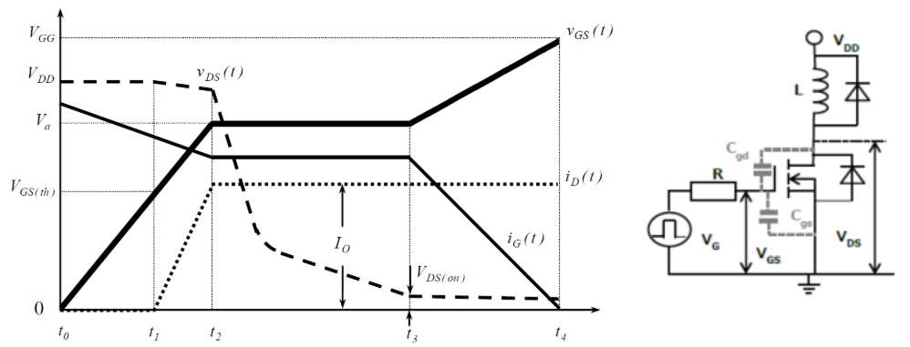
The MOS transistor D-pole load is an inductor plus a freewheeling diode, operating in the same mode as DC-DC BUCK. When the MOS transistor is turned on, the VDD charges the inductor L. Because the MOS transistor has a very short conduction time, it can approximate the inductor as a constant current source. When the MOS transistor is turned off, the freewheeling diode provides a discharge path to the inductor L, forming freewheeling.
The opening of MOSFETs can be divided into four stages:
Stage t0~t1
Starting from t0, the G pole charges the capacitor Cgs, and when Vgs rises from 0V to Vgs (th), the MOSFETs are in the cut-off state, Vds remains unchanged, and Id is zero.
Stage t1~t2
After t1, Vgs is greater than the MOS transistor turn-on voltage Vgs (th), and the MOS transistor begins to conduct. The Id current rises, and the equivalent circuit diagram is shown below. When the IDS current does not reach the inductor current, a portion of the current will flow through the diode, and the diode DF is still in a conducting state. The two terminals of the diode are in a clamp state, and at this time, the Vds voltage remains almost unchanged, with only a small decrease (due to the influence of stray inductance).

Equivalent circuit for stages t1 to t2
Stages t2 to t3
As the Vgs voltage increases, when the IDS current is the same as the inductor current, the MOSFET D-pole voltage is no longer clamped by the diode DF, and the DF is in a reverse cut-off state, so Vds begins to decrease. At this time, the driving current of the G-pole is transferred to Cgd for charging, and Vgs appears as a Miller plateau. The Vgs voltage remains unchanged, and Vds gradually decreases to the conduction voltage drop VF.
Equivalent circuit for stages t2 to t3
Stage t3~t4
When the Miller capacitor Cgd is fully charged, the Vgs voltage continues to rise until the MOS transistor is fully conductive.
Below, combined with the MOS transistor output curve, summarize the conduction process of MOS transistors.
T0~t1, the MOS transistor is in the cutoff region; After t1, Vgs exceeds the opening voltage of the MOS transistor. As Vgs increases, ID increases. When ID rises to the same level as the inductor current, the freewheeling diode reversely cuts off. During the t2~t3 time period, Vgs enters the Miller plateau period. At this time, the D-pole voltage is no longer clamped by the freewheeling diode, and the clamping area of the MOS becomes smaller. After t3, it enters the linear resistance area, and Vgs continues to rise. Vds gradually decreases until the MOS transistor is fully conductive.

MOS transistor output curve
Source: 21ic official account
Address: Block 2, No. 70, Yaofeng West Road, Wuzhong District, Suzhou City, Jiangsu Province
Tel: 0512-82285066
Email: sales@kegasia.com
Please contact us

WeChat official account
Copyright © SUZHOU KEG ELECTRONICS CO.,LTD All right reserved ICP NO:08120300-1 (Jiangsu) Technical support:Web design
![]()